Silicon Wafer Inspection with CMOS Image Sensor
Electronics play an integral part in our daily lives. Whether it be the phone you use, the car you drive or the computer you work on, we heavily rely on the technology that surrounds us every day.
The inner circuitry of these electronics requires a variety of metals and materials to properly function, with silicon being one of the most important components. Silicon is found in nearly every electronic device due to its unique properties in conducting electricity while also being an insulator depending on the conditions put on the silicon. As a key part of the quality control process, it is important to assess the quality and condition of the silicon-based semiconductors within technology. Silicon wafer inspection is the process of analyzing silicon material for any imperfections that may have occurred during fabrication.

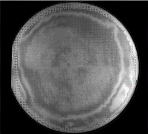
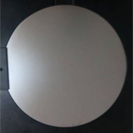
Similar to how humans require x-rays to view beyond our skin, shortwave infrared light acts as an X-ray for silicon wafers. At wavelengths beyond 1050nm, silicon is rendered transparent, which allows quality control technicians to inspect the silicon wafer for any clear cracks or damage.
Traditionally, expensive InGaAs sensors are used for silicon inspection as they can detect far beyond the 1050nm threshold. Although this technology works, the specialized manufacturing processes and expensive materials required to produce InGaAs sensors can make them a significant investment. As the global semiconductor market’s CAGR is expected to grow above 7% until 2027, there is an increasingly higher demand for cost effective quality control measures to keep up with semiconductor market demands. SeeDevice’s QMOS™ technology addresses this concern by utilizing quantum mechanics to see beyond traditional CMOS sensor limitations, into the SWIR range, offering a cost effective and powerful sensing solution for the future of silicon wafer inspection.


| Visible Light | SWIR Light |
About SeeDevice Inc.
SeeDevice is a fabless image sensor development company empowering the next generation of smart devices with its patented QMOS™ (Quantum effect CMOS) SWIR image sensor. SeeDevice’s sensor can send high-fidelity image data to AI vision systems and monitoring devices. QMOS™ delivers an industry-leading ultra-wide spectral range and among the highest infrared sensitivity by using innovative quantum pixel technology to advance CMOS process sensors.


